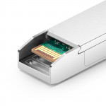
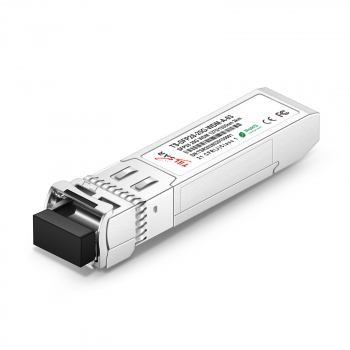
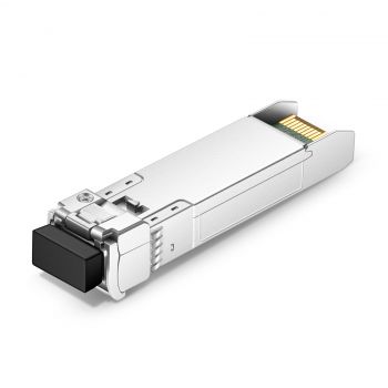
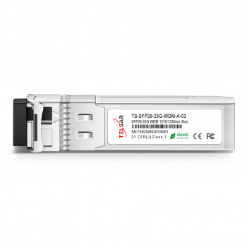
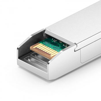
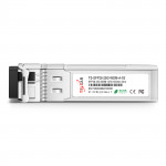
Оптический модуль TS-SFP28-25G-WDM-A-20 TELSAR форм-фактора SFP28 предназначен для передачи данных в одномодовом оптическом волокне (SMF) со скоростью до 25 Гбит/с на максимальную дальность до 20км. Рабочая длина волны 1270нм на передачу и 1330нм на прием сигнала, оптический бюджет 11 дБ, тип лазера: DFB. Модуль оснащен разъемом LC, поддерживает функцию Digital Diagnostics Monitoring (DDM) для контроля параметров производительности в реальном времени. Соответствует стандартам SFF8472, SFF-8431, SFF-8432.
Модуль TS-SFP28-25G-WDM-A-20 TELSAR предназначен для работы в паре с TS-SFP28-25G-WDM-B-20 TELSAR, но может также работать и с другими оптическими модулями SFP28 с обратным WDM делением длин волн приема/передачи.
Прошивка: CISCO. Если Вам требуется другая прошивка, сообщите об этом менеджеру перед заказом модулей.
- Сертификация лазерной безопасности Класса 1
- Скорость передачи данных до 25,78 Гбит/с
- Дальность передачи до 20 км
- DFB-лазер, высокочувствительный PIN-фотодиод и трансимпедансный предусилитель (TIA)
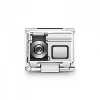
- Симплексный (одинарный) оптический разъем LC
- Разъем с возможностью «горячей» замены
- Низкое энергопотребление менее 1,5 Вт
- Широкий диапазон рабочих температур: от 0 до +75 °C
- Питание от одного источника +3,3 В ±5%
- Соответствие стандарту SFF-8472
- Полное соответствие экологическим директивам RoHS
Table 1: Transceiver pin descriptions
|
Pin
Number
|
Symbol
|
Name
|
Description
|
|
1,17,20
|
VeeT
|
Transmitter Signal Ground
|
These pins should be connected to signal ground on the host board.
|
|
2
|
TX Fault
|
Transmitter Fault Out (OC)
|
Logic “1” Output = Laser Fault (Laser off before t_fault) Logic “0” Output = Normal Operation This pin is open collector compatible, and should be pulled up to Host Vcc with a 10kΩ resistor.
|
|
3
|
TX
Disable
|
Transmitter Disable In
(LVTTL)
|
Logic “1” Input (or no connection) = Laser off Logic “0” Input = Laser onThis pin is internally pulled up to VccT with a 10 kΩ resistor.
|
|
4
|
SDA
|
Module Definition
Identifiers
|
Serial ID with SFF 8472 Diagnostics Module Definition pins should be pulled up to Host Vcc with 10 kΩ resistors.
|
|
5
|
SCL
|
|
6
|
MOD-ABS
|
|
7
|
RS0
|
Receiver Rate Select (LVTTL) Transmitter Rate Select (LVTTL)
|
These pins have an internal 30kΩ pull-down to ground. A signal on either of these pins will not affect module performance.
|
|
9
|
RS1
|
|
8
|
LOS
|
Loss of Signal Out (OC)
|
Sufficient optical signal for potential BER < 1x10-12= Logic “0” Insufficient optical signal for potential BER > 1x10-12 = Logic “1” This pin is open collector compatible, and should be pulled up to Host Vcc with a 10kΩ resistor.
|
|
10,11,14
|
VeeR
|
Receiver Signal Ground
|
These pins should be connected to signal ground on the host board.
|
|
12
|
RD-
|
Receiver Negative DATA Out (CML)
|
Light on = Logic “0” Output Receiver DATA output is internally AC coupled and series terminated with a 50Ω resistor.
|
|
13
|
RD+
|
Receiver Positive DATA
Out (CML)
|
Light on = Logic “1” Output Receiver DATA output is internally AC coupled and series terminated with a 50Ω resistor.
|
|
15
|
VccR
|
Receiver Power Supply
|
This pin should be connected to a filtered +3.3V power supply on the host board. See Figure 3.Recommended power supply filter
|
|
16
|
VccT
|
Transmitter Power Supply
|
This pin should be connected to a filtered +3.3V power supply on the host board. See Figure 3.Recommended power supply filter
|
|
18
|
TD+
|
Transmitter Positive DATA
In (CML)
|
Logic “1” Input = Light on Transmitter DATA inputs are internally AC coupled and terminated with a differential 100Ω resistor.
|
|
19
|
TD-
|
Transmitter Negative
DATA In (CML)
|
Logic “0” Input = Light on Transmitter DATA inputs are internally AC coupled and terminated with a differential 100Ω resistor.
|
Absolute Maximum Ratings
|
Parameter
|
Symbol
|
Unit
|
Min
|
Max
|
|
Storage Temperature Range
|
Ts
|
oC
|
-40
|
85
|
|
Relative Humidity
|
RH
|
%
|
0
|
95
|
|
Maximum Supply Voltage
|
Vcc3
|
V
|
-0.5
|
4.0
|
Recommended Operating Conditions
|
Parameter
|
Symbol
|
Unit
|
Min
|
Typ
|
Max
|
|
Operating Case Temperature Range
|
Tc
|
oC
|
-40
|
|
85
|
|
Power Supply Voltage
|
Vcc
|
V
|
3.14
|
3.3
|
3.46
|
|
Bit Rate
|
BR
|
Gb/s
|
|
25.78
|
|
|
Bit Error Ratio
|
BER
|
|
|
|
5*10-5
|
|
Max Supported Link Length
|
L
|
Km
|
|
|
20
|
Electric Ports Definition
|
Parameter
|
Symbol
|
Unit
|
Min
|
Typ
|
Max
|
Note
|
|
Supply Voltage
|
VCC
|
V
|
3.14
|
3.3
|
3.46
|
|
|
Power consumption
|
P
|
mW
|
|
|
1500
|
|
|
Transmitter
|
|
Input Differential Impedance
|
RIN
|
Ω
|
|
100
|
|
|
|
Single-ended Data Input Swing
|
VIN
|
mVp-p
|
90
|
|
450
|
|
|
Transmit Disable Voltage
|
VDIS
|
V
|
2
|
|
VCCHOST
|
|
|
Transmit Enable Voltage
|
VEN
|
V
|
VEE
|
|
VEE+0.8
|
|
|
Transmit Fault Assert Voltage
|
VFA
|
V
|
2
|
|
VCCHOST
|
|
|
Transmit Fault De-Assert Voltage
|
VFDA
|
V
|
VEE
|
|
VEE+0.4
|
|
|
Receiver
|
|
Single-ended Data Output Swing
|
VOD
|
mVp-p
|
200
|
|
450
|
|
|
LOS Fault
|
VLOSFT
|
V
|
2
|
|
VCCHOST
|
|
|
LOS Normal
|
VLOSNR
|
V
|
VEE
|
|
VEE+0.4
|
|
Optical Characteristics (Tc=-40 to 85 oC and Vcc= 3.14 to 3.46V)
|
Parameter
|
Symbol
|
Unit
|
Min
|
Typ
|
Max
|
Note
|
|
Transmitter
|
|
Nominal Wavelength (TS-SFP28-25G-WDM-A)
|
λ
|
nm
|
1260
|
1270
|
1280
|
|
|
Nominal Wavelength (TS-SFP28-25G-WDM-B)
|
λ
|
nm
|
1320
|
1330
|
1340
|
|
|
Average Output Power
|
Pav
|
dBm
|
0
|
|
6
|
|
|
Spectral Width (-20dB)
|
σ
|
nm
|
|
|
1
|
|
|
Extinction Ratio
|
ER
|
dB
|
3.5
|
|
|
|
|
Side Mode Suppression Ratio
|
SMSR
|
dB
|
30
|
|
|
|
|
Average Launch Power of OFF Transmitter
|
POFF
|
dBm
|
|
|
-30
|
|
|
Relative Intensity Noise
|
RIN
|
dB/Hz
|
|
|
-128
|
|
|
Receiver
|
|
Center Wavelength (TS-SFP28-25G-WDM-B)
|
λC
|
nm
|
1320
|
1330
|
1340
|
|
|
Center Wavelength (TS-SFP28-25G-WDM-A)
|
λC
|
nm
|
1260
|
1270
|
1280
|
|
|
Receiver Sensitivity
|
RSENSE
|
dBm
|
|
|
-13
|
1
|
|
Receiver Overload
|
Pmax
|
dBm
|
2.2
|
|
|
|
|
Optical Return Loss
|
|
dB
|
|
|
-26
|
|
|
LOS Assert
|
LOSA
|
dBm
|
-30
|
|
|
|
|
LOS De-Assert LOS
|
LOSD
|
dBm
|
|
|
-17
|
|
|
LOS Hysteresis
|
|
dB
|
0.5
|
|
|
|
Note1: Measured at 25.78125Gb/s,ER>3.5dBm, PRBS 231-1 and BER better than or equal to 5E-5;





 TELSAR - зарегистрированный товарный знак компании ООО «ТВБизнес»